Hacking the My Arcade Contra Pocket Player - Part I

Intro
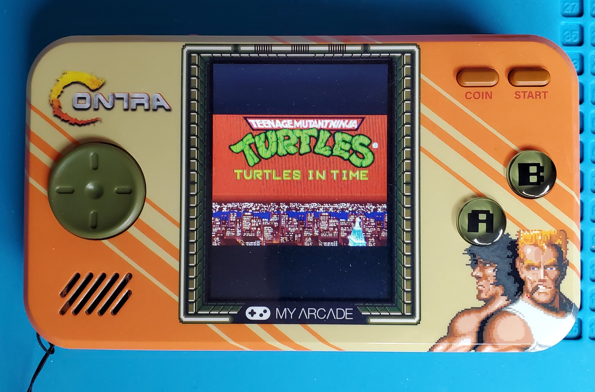
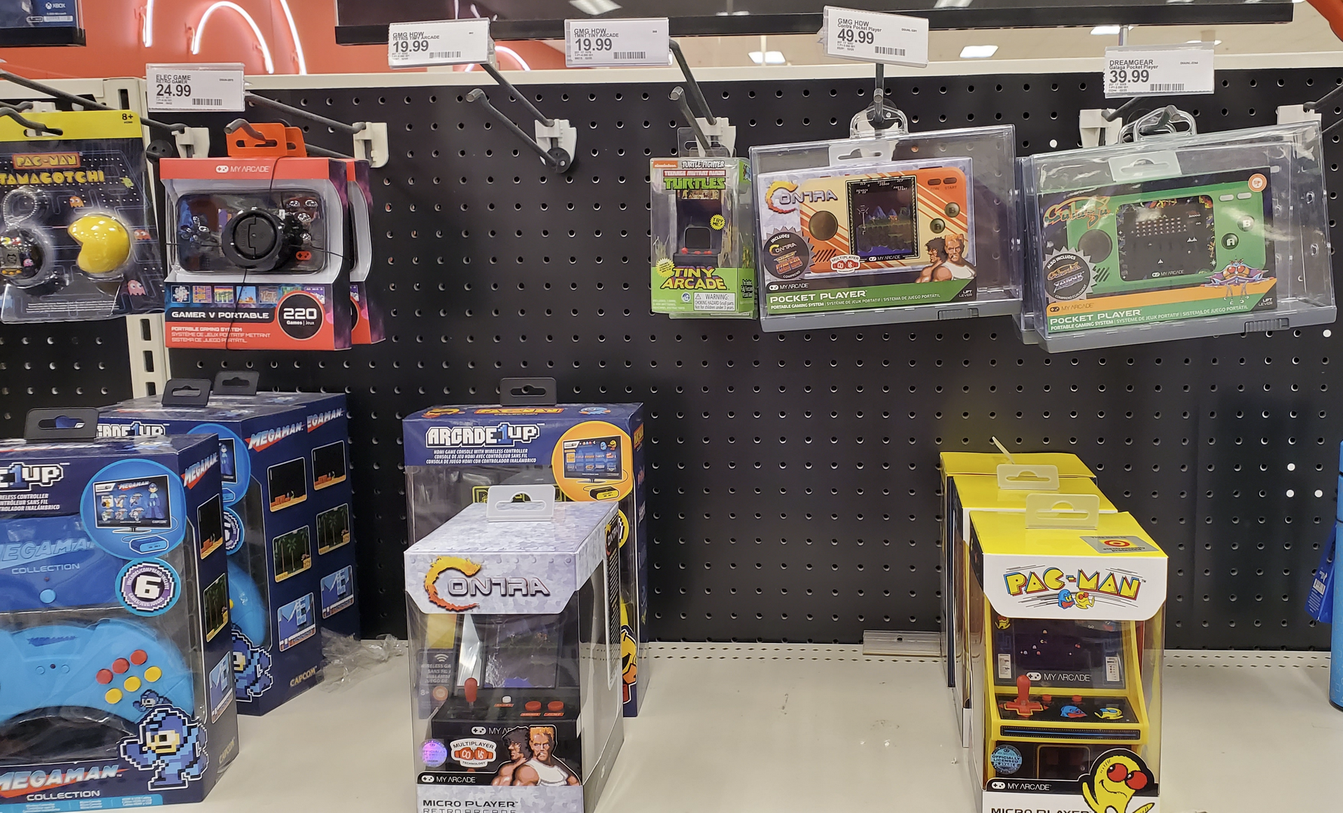
I was at my local Target recently and spotted the section near the video games, where there were some little collectable arcade systems and handhelds that play games like Pac-Man, Galaga, and Contra.
Whenever I see these types of systems, I like to pick one up to tear it apart and see what's inside. Often, the manufacturer uses what's known as a "NES-on-a-chip" or "Famiclone", which is a custom ASIC that mimics the NES hardware on a tiny chip, usually found under a black blob on the circuit board. The Famiclone systems are neat, and you might even be able to swap out the ROM on the flash storage, but it’s usually going to be limited to loading NES ROM or using the included terrible games that are basically hacked up versions of real NES games with all the sprites swapped out.
As I was looking over the options, this Contra handheld caught my attention for a few reasons…
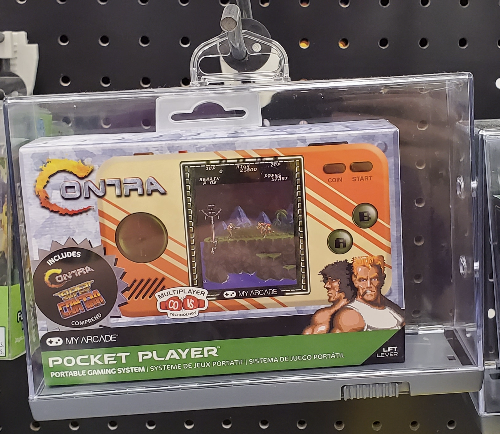
First, it advertises multiplayer compatibility using "CO/VS Technology". Second, I noticed that the screen was tall, like the arcade version of Contra, as opposed to a more 4:3 layout that would be expected from a system running an NES chip inside. At this point, I was intrigued enough to pick up a few of these handhelds for testing (and to remind myself how bad I am at this game).
Teardown
Inside the game console, there are multiple components of interest.
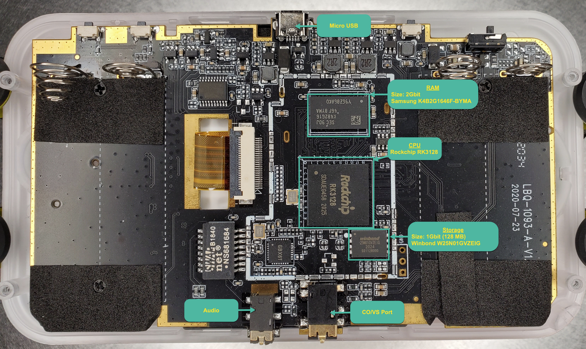
The device is using a Rockchip RK3128, which is a SoC consisting of a quad-core Cortex-A7 and Mali400 MP2 GPU. It has 2Gbit of DDR3 RAM and 1Gbit of storage. A Winbond serial NAND flash is used for storage, which is connected to the CPU via an SPI interface. There is a micro-USB port that can be used to power the device, an audio port, and the CO/VS port used for co-op/multiplayer with a second device.
Hardware Probing
Initially, my first thoughts after opening the device were to attempt to get a flash dump. Typically, I would reach for my HydraBus or Bus Pirate and flashrom to dump a flash device, but this storage chip is not supported. That is because flashrom is typically used to operate on SPI NOR flash, but the Winbond W25N01GVZEIG is a NAND flash.
With that in mind, I decided to take a read through the NAND flash datasheet to see how I could interface with this thing. Before we hook the flash up to the HydraBus, it is important to understand the NAND flash architecture so we can figure out how to properly dump the data.
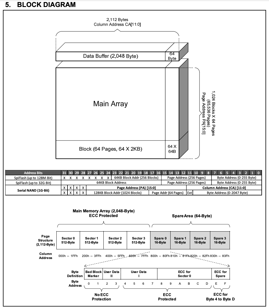
After reviewing the block diagram, we learn the following:
- The flash is organized by blocks
- Blocks consist of 64 pages
- A page consists of 2,112 bytes of data
- 2048 bytes of actual data
- 64 bytes reserved for ECC data
- A column address is used to index into the page to read specific bytes
So, to dump the data, we would need to load the first page into the data buffer, set the column address to the first bytes, and start reading. We should be able to increment the column address to read the whole page and then load the next page until we have read all of the pages.
Let's check the pinout to see how we should hook this up to the HydraBus.
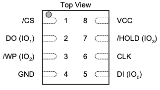
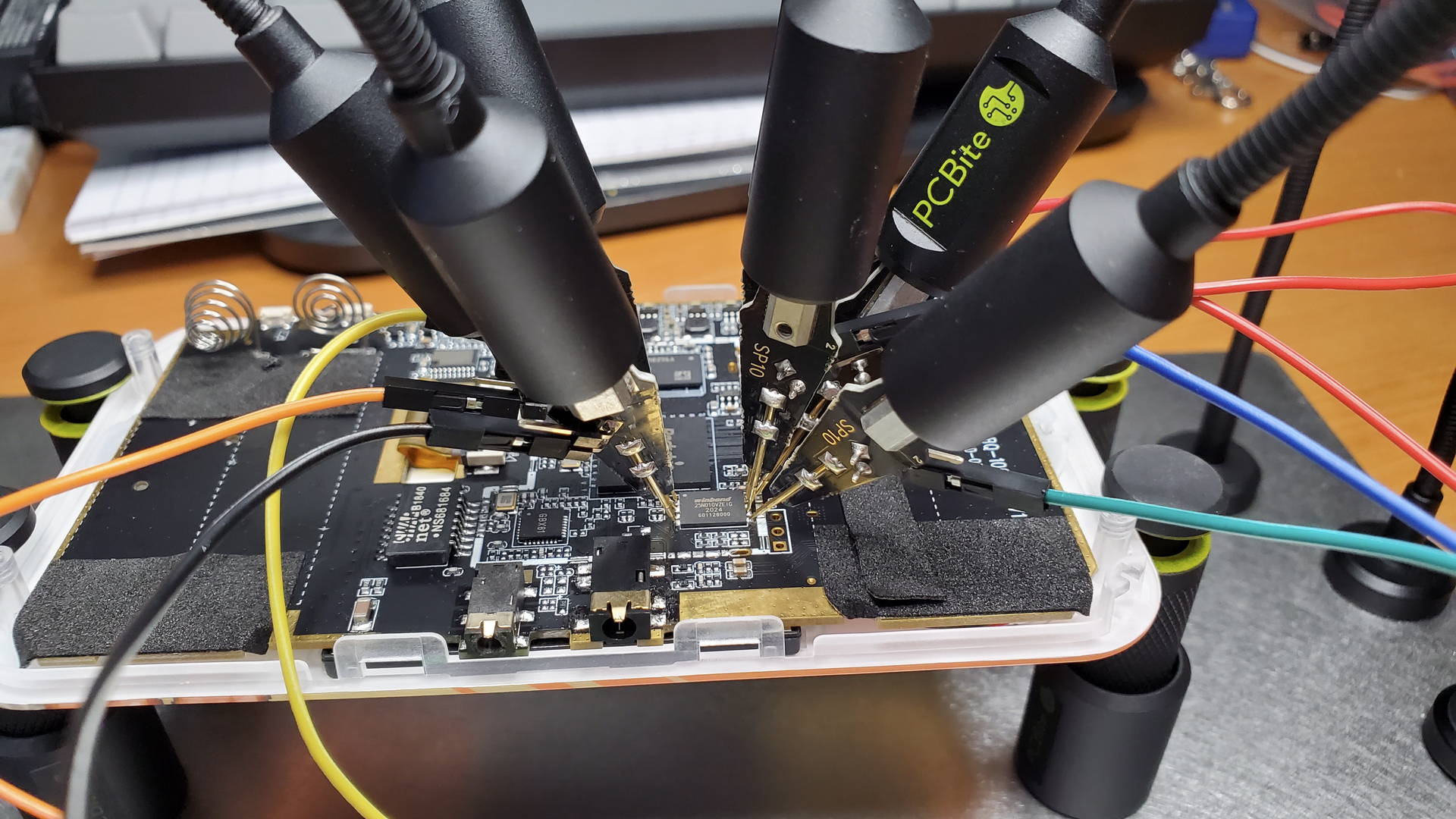
Since this is an SPI interface, it is straightforward to hook up. I'm using PCBite probes to make contact with the pins here, which works amazingly well and prevents me from needing to solder wires to the flash chip.
With everything hooked up, we can try to do a simple operation to make sure we have everything set up correctly. Most SPI memory chips should support the Read JEDEC ID instruction, which returns a few bytes that can be used to identify the flash chip.
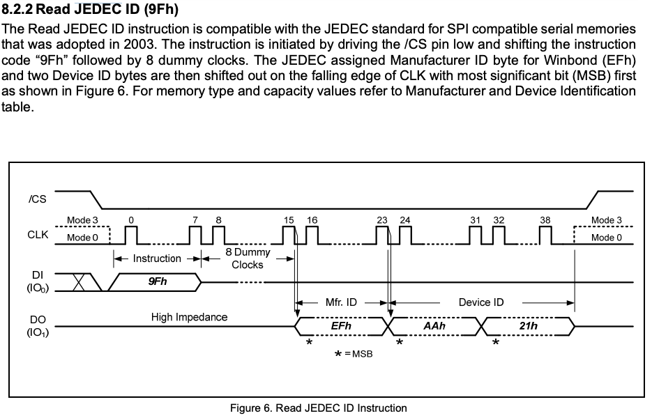
Reviewing the command in the datasheet, it seems we need to send a 0x9f followed by 8 'dummy' clocks. Since we will be transmitting 1 bit per clock cycle, that means we can send a 0x9F followed by any single byte to fill up the 8 clock cycles. We then need to read the following 3 bytes that will be shifted out.
Using the HydraBus, we can do this by entering into SPI mode and using the following command:
[ 0x9F 0x11 r:3 ]
Let's break down the command to see what we are doing here:
| Command | Description |
|---|---|
| [ | Chip Select (CS) enable (active when pin is low) |
| 0x9F | Send the Read JEDEC ID command |
| 0x11 | Dummy byte to fill 8 clock cycles (can be any byte like 0x00) |
| r:3 | Read the next 3 bytes sent from the NAND flash (this is out JEDEC ID) |
| ] | Chip Select (CS) disable (inactive when pin is high) |
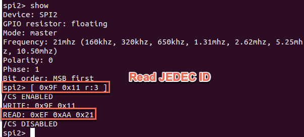
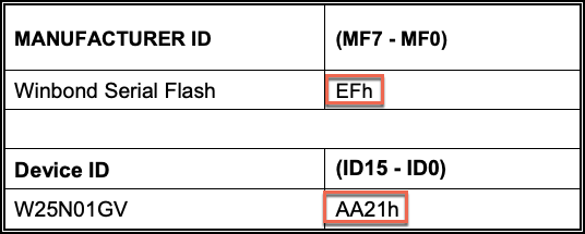
Cool, we got 0xEF 0xAA 0x21 as our result. Let's compare this with the Manufacturer and Device ID listed in the datasheet.
Great! It seems we were able to get the expected result back. At this point, we are ready to try dumping some data.
Dumping the Flash....Maybe...
[ 0x03 0x00 0x00 0x00 r:255 ]
Let's break down the command again:
| Command | Description |
|---|---|
| [ | Chip Select (CS) enable (active when pin is low) |
| 0x03 | Read the data command |
| 0x00 | Column Address CA[15:8] |
| 0x00 | Column Address CA[7:0] |
| 0x00 | Dummy byte to fill 8 clock cycles |
| r:255 | Read the next 255 bytes sent from the NAND flash |
| ] | Chip Select (CS) disable (inactive when pin is high) |
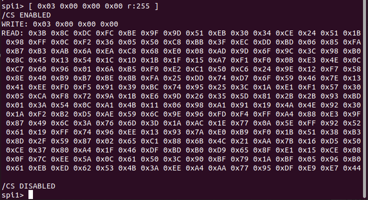
At this point, I thought I was getting good data. However, after a bit of experimenting, I noticed that attempting to read from the same location would occasionally return different data, and I was unable to reliably page through and read the NAND to assemble an accurate dump.
I'm not sure if the issue was due to attempting to read the NAND in circuit or if I had configured the HydraBus incorrectly. I could have attempted to debug the communication on a logic analyzer or oscilloscope to determine the issue, but I ended up not needing to go down this road, as it turns out there is a much better way to dump the data...
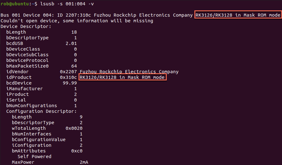
RTFM - USB Recovery
Doing a little bit of Google searching on the RK3128 chip revealed that it is commonly used in lower-end Android devices and TV boxes. There are multiple resources for many of these devices that suggest you can get into recovery mode by holding down the volume up key when powering on the device. This is even documented on the Rockchip wiki.
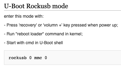
Sure enough, by powering on the device while plugged in via USB and holding down the volume up key, the device is detected as a RockUSB device in Mask ROM mode.
NAND Dump
At this point, we should be able to use rkflashtool, which speaks the RockUSB protocol to get a dump of the NAND storage.
However, before we can do that, we have just a little more work to do. rkflashtool expects the offset and size parameters in blocks of 512 bytes.
If we go back to the NAND datasheet, we can see that it contains 65,536 pages of data
with 2,048 bytes per page for a total of 134,217,728 bytes of data.
If we divide that by our sector size of 512 bytes, that gives us 262144 total sectors. Using this information, we should now be able to dump the entire NAND, starting at sector offset 0 and ending at sector 262,144.
sudo ./rkflashtool r 0 262144 > ~/Desktop/nand_dumps/nand_dump.bin
At this point, I usually like to attempt 1-2 additional dumps so I can compare the file hashes and see that we have a good clean dump.
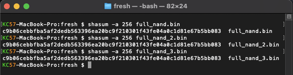
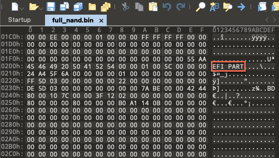
The hashes for each dump match, so we likely got a good dump here. We can see some interesting stuff near the beginning of the dump, including a GUID Partition Table header.
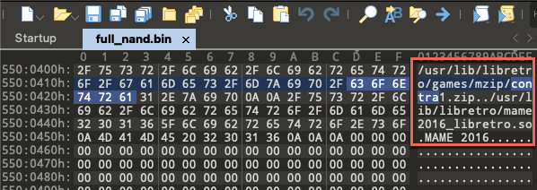
If we do a little searching, it looks like we found a reference to a Contra ROM and the arcade emulator MAME.
Part 2 Sneak Peek...
Stay tuned for Part II of this post, where we will dig into the NAND image, swap out the ROMs, and see what else we're able to get running on this thing!